Wednesday, August 24, 2011

Pratap Raychaudhuri: Phase fluctuations in 2D and 3D NbN thin films

Pratap Raychaudhuri gave a beautiful talk on their very systematic and complete measurements on various properties of NbN films. He started by reminding us that low superfluid density superconductors may have phase transitions which are driven by fluctuations of the superconductor's order parameter's phase. These fluctuations are largely irrelevant for conventional superconductors where the "phase stiffness" is 10^7 K. The phase stiffness is the energy scale to put twists in the superconducting phase. In highly disordered systems or in systems where otherwise the superfluid density is low, the stiffness can be of order T_c.

Their material of choice is NbN, which is claimed to be a garden variety type II crystalline superconductor. They sputter epitaxial films and although films are largely crystalline, they can control defects and hence disorder in the materials by controlling the ratio of Nb to N2 in the plasma.

Pratap then gave us a brief review of the physics of the KTB transition. He reminded us about universal jump of the superfluid density in which there is a discontinuous jump of the superfluid density of an amount set by the transition temperature itself.

They measure superfluid density (or phase stiffness) that they parametrize by inverse penetration depth squared. They observe that in thin nominally 2D films the inverse penetration depth shows a substantial downturn in the rough vicinity of the KTB expectation, although the downturn has a magnitude is systematically less than T_KTB. They perform a detailed fitting based on a model which takes into account the finite vortex energy and a small distribution in superfluid densities and get energies of order the expectation for vortex core energies of order the expectation for 2DXY model.

Pratap then moved to samples which are more 3D. They get k_Fl from Hall and DC resistivity measurements. They find that T_c goes to zero around the disorder level where kFl approaches 1, which is essentially indistinguishable from the disorder level where the normal state conductivity is going to zero. i.e. the MIT is coincident with the SIT.

Pratap then discussed their STM results. He showed line scans on a variety of films. For instance on low disorder film the sample shows a large BCS-like gap which don't depend on position and opens up at T_c. He then showed data from more disordered samples. These samples show an onset in superconducting features in the tunneling spectra above T_c. For the particular sample he concentrated on T_c was ~2.5 K and his T* was 7-8K.
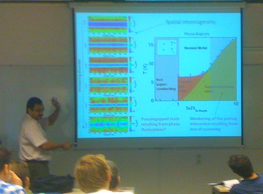

Then he showed a phase diagram as a function of k_Fl. For high k_Fl, T* and T_c coincide, but as k_Fl approaches 1, then T* and T_c separate and there is a substantial pseudogap (PG) regime. This is the same regime where T_c is suppressed to zero. He then asked if it was reasonable to assume that in this regime the transition was driven by phase fluctuations. To answer this question, he then presented their penetration depth data which was taken on these same samples. On the samples with a substantial PG the phase stiffness is of order T_c.

In the last part of the talk he analyzed the BCS prediction for the phase stiffness for samples with these T_c's (Blogger: same spectral weight in the superconducting condensate). He showed that for highly disordered samples the phase stiffness was systematically less than the BCS expectation. He attributed this to quantum fluctuations of the superconducting phase.

In the future, they want to look for low energy dissipative modes (which derive in their interpretation from quantum fluctuations) via microwave measurements. In the tunneling spectra they see low energy in-gap states for highly disordered samples and Pratap mentioned that perhaps these were the low energy modes. (It was not clear to the blogger how this was relevant, as tunneling measures single particle excitations and presumably these modes are not single particle excitations.).

As one final final point, he mentioned that for 3D samples which were just barely disordered enough not to be superconducting, they see a large magnetoresistance peak as has been see in materials ilk TiN and InO. He interpreted this peak as the delocalization of Cooper pairs.

In the questions, the blogger pointed out that one could get a depleted condensate density (lower phase stffness) by inhomogeneous superfluid density alone. Then by arguments of spectral weight conservation one must have finite omega plasmon-like modes. These are purely classical (or at least not necessarily quantum) and so are really a different effect than the one Pratap discussed, but in principle could also explain his data.

Blogged by Peter Armitage

Tuesday, August 23, 2011

Zvi Ovadyahu: Field-enhanced conductivity in electron-glasses

Zvi Ovadyahu reported on the absorption rate in strongly localized Anderson insulators.

The bottom line message of the talk was to provide evidence that the electron-electron inelastic scattering rate in Anderson insulators is strongly suppressed from its value in the less disordered, diffusive regime. This may be an indication of the physics of many-particle localization in strongly disordered systems.

The material under investigation was InOx, one of the standard materials in which electron glassiness is studied. An electron glass is an Anderson insulator where all relevant single particle states are localized. Coulomb interactions are very important due to the absence of standard screening. Thus there are strong and long ranged interactions, as far as screening due to gates or thermal excitations can be neglected. The frustration between disorder and Coulomb interactions produces a glassy state.

All samples studied for the present purpose were 2d, crystalline In2O{3-x} films, measured at 4K where they are in the hopping regime (resistances ~10 MOhm). This specific variety of InOx was chosen because all its parameters are known, being close to a free electron system (unlike the amorphous systems).

The basic glassy or out-of-equilibrium phenomenon in InOx is the slow logarithmic relaxation of conductance with time after a quench from high T. Other ways to excite the system include non-Ohmic fields, or raising the bath temperature, both of which make the conductance quickly jump upwards, and then slowly increase further. Upon undoing the perturbation the conductance jumps down and relaxes back logarithmically towards the previous state. Both excitations have qualitatively similar effects.

The system was excited with non-Ohmic fields of various frequencies, to pump energy into the system. Thereby the power was adjusted in such a way as to keep the initial jump of conductance constant. The frequency range covered 23 Hz up to15.5 MHz.

A first interesting result concerns the apparent energy, as a proxy for which the initial conductance after the downjump is taken. Apparently, the absorbed energy depends on the frequency: it starts decreasing for frequencies of order 10^5 Hz and higher. The meaning of this characteristic scale frequency was not explored further here.

The focus of the talk was rather on the rate of e-e inelastic processes. An upper bound for the latter was obtained by considering the heat balance in the steady state under non-Ohmic excitation. This allows to obtain a good estimate of the heat removal rate from the electrons. Ovadyahu argues that in the steady state, it must be an upper bound on the inelastic collision rate, which controls absorption (otherwise the system would absorb more energy and come to a steady state with higher heat removal rate). His finding is that the inelastic rate in the insulator is as small as gamma= 3.5*10^5 Hz, as compared to measured rates of the order of 10^11/s in the diffusive regime.

The large difference must almost inevitably be blamed on localization and the associated discreteness in the insulator (the single particle level spacing is 100-10^4 K!). From this point of view the experiments seem to be consistent with tendencies expected in systems featuring manybody localization, as proposed by Basko et al.. Remarkably, the (near) discreteness seems to hold despite the presence of strong, long range interactions, which are in principle expected to destroy the discreteness of the spectrum and delocalize the many body excitations (see, Fleishman and Anderson).

A possible element of an explanation may be that these excitations are indeed delocalized, but have a very low diffusivity because dipolar interactions in 3d are only marginally long range which is the case of critical hopping, discussed in Anderson '58.

Blogged by Markus Mueller

Jian-ting Ye: Liquid-gated interface superconductivity on an atomically flat film

Jian-ting Ye discussed their recent beautiful work from Tokyo on gating various materials to induce superconductivity (and other states of matter) using ionic and organic electrolyte solutions. They make an electronic double layer transistor (EDLT) with liquid gating. Much more charge is introduced as compared to conventional SiO2 style dielectrics.

Jiang-ting discussed a large number of results using this technique. With polymer electrolyte solutions, they have found a 2D metal-insulator transition in ZnO. (As a practical matter, states induced by this method will generally be 2D) For smooth changes of voltage, there is a sudden onset in resistance when resistance gets near h/e^2. They have also induced superconductivity in StTiO3 around 0.4K, which is a similar temperature to that found recently in STO/LaAlO3 superlattices. Capacitance is high enough that for materials like graphene they can see particular bands crossing the Fermi level in the case of graphene.

To get larger charge densities they use ionic liquids where they get get ~ 20 times higher charge density than with polymer electrolytes. They have looked at many layered structures (cuprate superconductors, layered chalcogenide topological insulators, layered chalcogenide superconductors, etc.) and found a number of effects. But in the rest of talk will talk he was going to emphasize their work on superconductors.

ZrNCl was induced to be a superconductor at 15.2K with Tc's very similar to what is found when this material is doped with Li.

Transition metal chalcogenide MoS2 when electron doped with the EDLT technique is found to have superconductivity at 9K. This is higher than the previous record of about 6.5K when this system is doped with alkali metals. They also find ambipolar conductivity for positive and negative bias in this system, but no ambipolar superconductivity yet.

It was asked by Finkelstein why it is that there is is no problem with mobility in these systems, in the sense that in 2D electron glass in semiconductor heterostructures, dopant layers reduce mobilities. Why does not this not happen here? The speaker replied that they are in a different regime with regard to the range of mobilities. Here mobilities are in the 100's at best, whereas the best 2DEG have mobilities 10^4.

Blogged by N. Peter Armitage

Jim Valles: Insulator to superconductor transitions come in multiple flavors in quench condensed films

Jim Valles describes that superconductor to insulators transitions (SIT) come in 3 flavors in quenched condensed films: granular, uniform and nano-honecomb (NHC) structures. The NHC films usually have the thickness about the same as the uniform ones and the variation in their thickness is about a couple of angstroms.

Jim Valles discussed the possible ways to kill the superconducting order parameter through SIT. In weakly localized system, the transition happens in an amplitude reduction fashion and cooper pairs (CPs) are de-paired. Another way to kill superconductivity is phase fluctuation which leads to localized CPs. In granular films, quasi-particle (qp) tunneling dominates while for NHC films, CPs tunneling takes charge.

For quenched condensed Bi films, with a-Sb underlayer, those films on glass or AAO (honeycomb structure) substrates are homogeneous, while the films are granular when the underlayer is missing. Most of the Bi measurements have to be done in situ.

He explained how resistance evolves in granular films through SIT and those films tend not to be conducting unless one has 2 layers of grains. Granular films usually have localized CPs and phase fluctuations near SIT. The transport effects are dominated by interisland qp tunneling. He showed data for granular lead which has giant negative magnetoresistance(MR) and can be fitted to SIS model with magnetic field induced pair-breaking.

For uniform amorphous Bi film, he thinks they are in the Fermi insulator phase. For weak insulating normal state, the change in conductance is proportional to log(T). They have positive but not large MR. Superconducting gap also disappears near SIT and the energy gap can be fit roughly with BCS form. Reference Valles, Dynes, Garno PRL 1992.

For NHC Bi films, perpendicular penetration length is about 1 mm and coherence length is about 10 to 20 nm. AFM images of this type of samples show “regular” height +variation. Thickness tuned SIT shows re-entrant behavior. NHC insulating films has a hard gap R~R0 e^(T0/T) and the activation energy T0 goes to 0 for thicker films. They exhibit large flux oscillation under perpendicular field and also giant positive MR. Transport measurements are dominated by incoherent CP tunneling. The size of the orbit of CP is dictated by the size of the unit cell. He believes that for NHC Bi films, they have phase fluctuations driven SIT and localized CPs do exist.

He raised a couple of questions about the origin of the activation energy, origin of giant MR, the mechanism causing localized CP in NHC films and also why qp/CP tunneling dominated for granular/NHC films.

He answered some of the above questions by introducing a local Tc0 variation which is caused by thickness variations in NHC films. He mapped out Tc as a function of position near SIT and introduced a weak link model. By including a circuit model, he got R^(link) at the critical point to be R_Q.

Blogged by Wei Liu (JHU)

Claire Marrache-Kikuchi: Thickness, composition and annealing tuned disorder in NbxSi1-x

Claire Marrache Kikuchi gave a detailed presentation on disordered amorphous NbxSi1-x focusing on 3 different ways to control disorder: (i) By tuning the thickness of the sample, (ii) by changing the composition and (iii) through controlled annealing. She started by reminding the audience that different kinds of disorder can have fundamentally different effects. For example, with decreasing thickness surface phonon softening can play an important role and has often been argued to be the reason for enhancement of T_c in observed in Al and Sn. In addition, she reminded the audience, the difference between homogeneous and granular disorder has been highlighted by many authors.

Amorphous thin films of NbxSi1-x were grown through co-deposition of Nb ans Si using electron beam evaporation. For thick films (thickness>50nm) samples with composition 11-18% Nb showed superconductivity. The samples have electronic density of states at Fermi energy in the range 1041 states/J-cm3 which is comparable to that of Au. TEM images of the samples do not show any granular structure.

The composition tuned samples have a metal-insulator transition at 9.9% of Nb, with samples below this composition range exhibiting Efrot-Schlovsky behavior in their transport properties. Interestingly, in this system superconductivity gets apparently destroyed well inside the metallic regime unlike amorphous InOx and TiN where superconductivity persists in the disorder driven insulating regime. This point towards a very different mechanism, arising maybe from the increase in e-e interactions resulting from a loss of effective screening, which drives the superconducting transition temperature in this material. However, further measurements down to lower temperatures would be needed to confirm this.

In the composition range where the samples are superconducting (e.g. 14%, 15% and 18%), Tc monotonically decreases with decresing thickness. The dependence of Tc on the sheet resistance is qualitatively consistent with an increase in e-e repulsive interaction resulting from the loss of effective screening. However, there are quantitative discrepancies with theory.

The most intriguing aspect of these samples was the effect of annealing. While there is no discernible change in the morphology with annealing up to 5000C, contrary to usual expectation the sheet resistance gradually increases and the Tc decreases with increasing annealing temperatures. There was considerable discussion on the microscopic changes that could be responsible for this behavior. It was felt that this issue needs to be looked into further using other microscopic tools. However, one important point was that Tc evolves in the same way with sheet resistance for both composition driven and annealing driven disordered sample, whereas the thickness tuned samples did not fall on the same curve.

In summary, the well characterized samples of NbxSi1-x would definitely provide us with another system where various scenarios proposed for the superconductor-insulator transition could be compared with experiments. It would be interesting to study these sample with various experimental probes such as STM and penetration depth measurements and compare the commonalities and differences with TiN, NbN and InOx. Prof. Claude Chapelier mention during the discussion that STM measurements on this system are underway. Hopefully, as more systems get studied, a common picture for the disorder driven SIT in various systems will gradually emerge.

blogged by Pratap Raychaudhuri

Teun Klapwijk: Highly resistive superconducting resonators: why and how


Teun Klapwijk spoke on energy-resolving THz detectors for astrophysical
observations. These frequencies are of interest for learning about the early
universe, some 400 million years ago, where radiation from the first stars
excites nearby dust, which then re-radiates in the THz band (~100-600 micron
wavelength).

Previous cryogenic detectors used for this purpose are TESs, photon-assisted
tunneling devices (SIS junctions), and HEB mixers.
in photon-assisted tunneling detectors, an SIS junction is voltage biased
such that THz photons can create quasiparticles above the gap by direct
absorption. HEB mixers use the self-heating-induced nonlinearity in a
nanoscopic superconducting microbridge to mix THz radiation down to
microwave frequencies. TESs use a very sharp resistive transition in a very
low-Tc material as a thermometer to detect the temperature change of a very
low heat-capacity, well-isolated absorber due to the absorption of single
photons.

TESs are the most advanced of these and have the world-record low
noise-equivalent power of ~10^-20 W/Sqrt[Hz] (Gershenson). This has now
reached the limit associated with the background photons, below which
further increases are less useful.

However, one disadvantage of these detectors is that they are read out with
SQUID amplifiers, which are difficult to read out in extremely large
numbers. The most advanced TES array for this purpose, SCUBA II, has 10000
array elements.

Microwave kinetic-inductance detectors have a possibility to go beyond this
limitation. They are built out of extremely high-Q resonators of disordered
superconducting films, with high kinetic inductance and broadband
absorption. Absorption of a photon generates quasiparticles which both shift
the resonator frequency (due to the modified kinetic inductance) and reduce
the Q (due to additional dissipation). This can be detected my monitoring
the microwaves reflected from the resonator. In addition, many resonators
can be connected to the same feedline in parallel, each with a slightly
different resonance frequency. As the Q is increased, the density of these
frequencies can also be increased, up to the required bandwidth for the
detector elements. This allows many detector elements to be read out on a
single coax, so that very large arrays can be contemplated without requiring
impractically many coaxes.

The figure of merit for an MKID involves several factors. First, the
fraction of the total inductance in the resonator which is kinetic; ideally
this would be 1 for maximum sensitivity, and this suggests the use of very
high kinetic inductance materials and geometries. Second, the quasiparticle
recombination time, which should be as long as possible, such that a given
number of excitations can be measured for maximum time in the resonator.
Third, the resolator Q should be as high as possible, in order to be
sensitive to as small an inductance change as possible. Finally, the
quasiparticle density of states should be as low as possible, for maximum
fraction change in the kinetic inductance for a given number of
quasiparticles.

TiN maximizes these figures of merit in many ways better than any material
previously tried:
- The high sheet resistance corresponds to a very high kinetic inductance,
giving kinetic inductance fractions near unity, and very compact resonators.
- Extremely high Q values up to 2 x 10^7 have been demonstrated at high
power
- The Tc can be continuously tuned by varying the deposition parameters;
this allows low gaps to be used for maximum sensitivity
- The extreme disorder gives very good far-IR absorption
- In spite of the high disorder, the quasiparticle lifetime is still
reasonably long

Blogged by Jamie Kerman

Vincent Bouchiat: Tunable 2D superconductivity in metal-decorated graphene

Bouchiat presented experimental results from recent transport studies on superconductivity in thin metals deposited on top of 2D graphene layers. Gated graphene is used as 2D host material mediating interactions between adsorbed metal islands. These metal islands both efficiently dope the underlying graphene sheet and induce long range superconducting correlations.The fabrication of these systems were done in collaboration with Zettl's group at Berkeley. The dewetting of metals such as Pb, In, Sn when deposited on graphene allows non percolating islands of adsorbates to be formed on graphene with typical sizes of ~ 50 nm with inter-adsorbate distances ~ 80 nm (for Sn). With Sn islands on graphene, a gate-induced superconductor-normal transition was observed. When plotting resistane vs temperature, two drops in R are observed: one at T_c, corresponding to the bulk superconducting transition in the clusters and a second one below T_c, at T_BKT, where vortex unbinding occurs. By tuning the gate voltage and thereby the carrier density in the graphene sheets, it is found that T_c remains constant but T_BKT can be tuned on both the electron and hole branches on either side of the charge neutrality point in graphene.

In the second part of the talk, more disordered graphene layers grown by CVD method is used to study Pb clusters. The interesting results are: (1) Dirac point is found to be an insulating point and (2) superconductivity in found only on one side of the charge neutrality point. A gate-tunable superconductor-insulator transition was observed and the graphene layer was found to act as both Josephson and dissipation channels.

In summary, in clean exfoliated graphene, a gate controlled 2D superconductivity - BKT transition was observed and in disordered CVD grown graphene, a gate-controlled superconductor-insuator transition is observed. Metal decorated graphene appears to be a useful model system to study gate-controlled superconductivity. Some results presented have appeared in Phys. Rev. Lett. 104, 047001 (2010).

Blogged by Sambandamurthy (Buffalo)